
|
PCB design
-
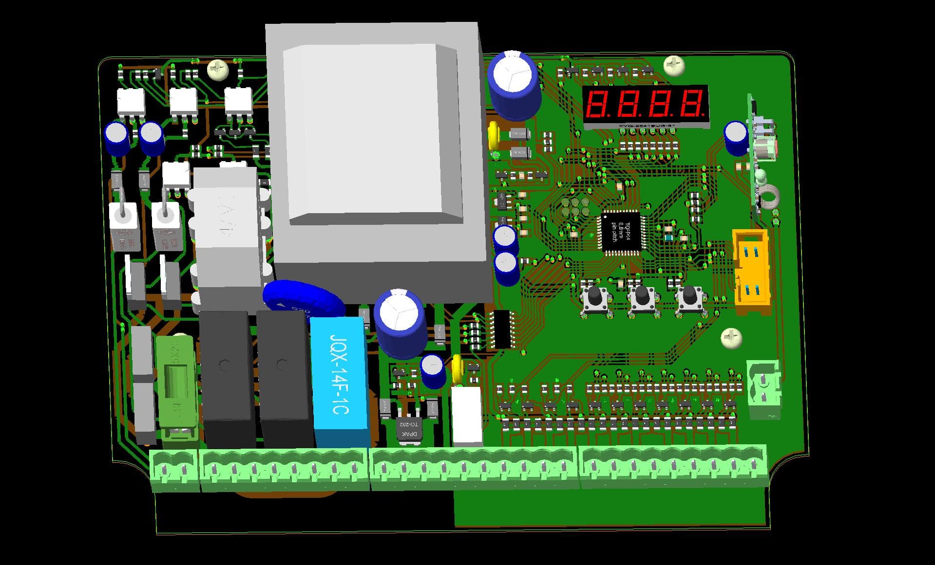
PCB design in OrCAD Cadence 16.2 or 3D OrCAD PCB Designer Professional 16.6.
-
Design complexity and number of layers are not limited in fact, HDI technology - stacked mikroVIAs,
drilled holes from 0,1mm, blind-VIAs and buried-VIAs.
-
Color of solder mask on demand - green, blue, black, white.
-
Possibility of applying a protective coating - spray against the effect of moisture.
-
Lead and lead-free HAL, chemical tin, chemical Ni/Au, galvanic Ni/Au.
-
Express terms of design and production according to customer requirements.
-
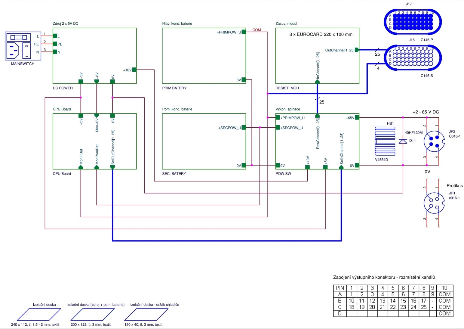
Documentation creation with cross-page links - also suitable for large electronic assemblies.
-
Easy import of design to mechanical 3D CAD tool via design step model.
-
Mounting technology - thruhole, SMT and combined.
-
Long term cooperation with czech and international customers.
-
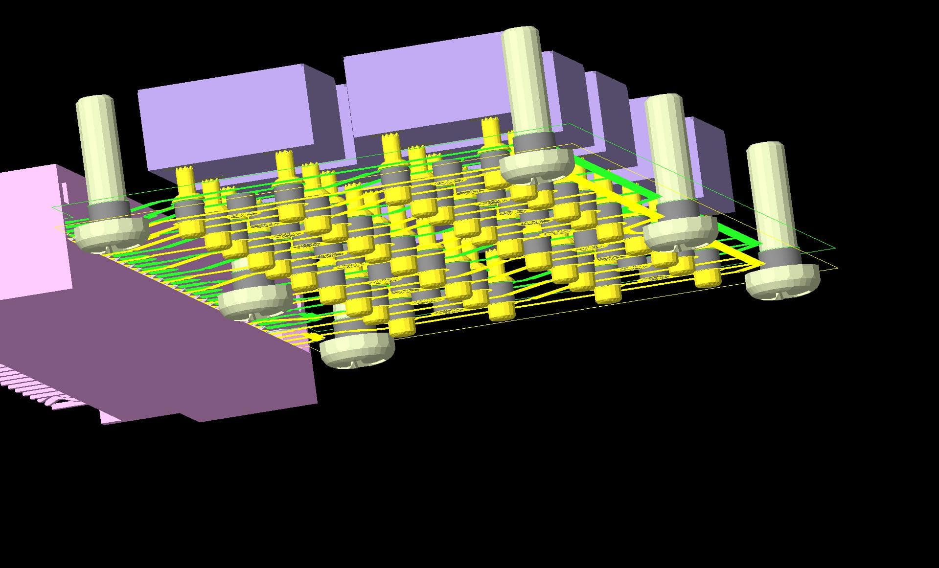
Design and manufacture of special jigs for testing of electronic components.
-
Long term practice with mechanical construction - many special parts can be
designed and effectively produced in PCB technology.
3D design, part of construction
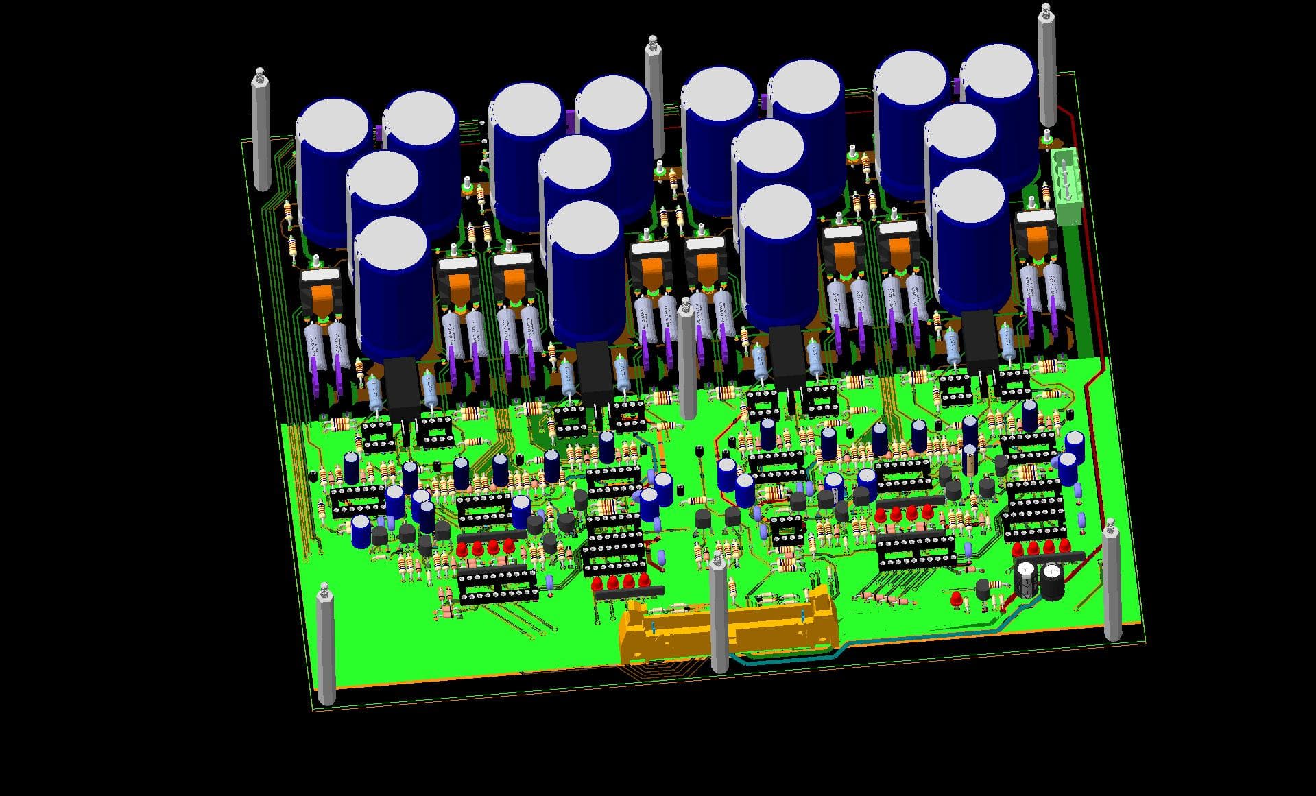
3D design, part of construction
3D design of special jig
3D design with BGA and WLCSP
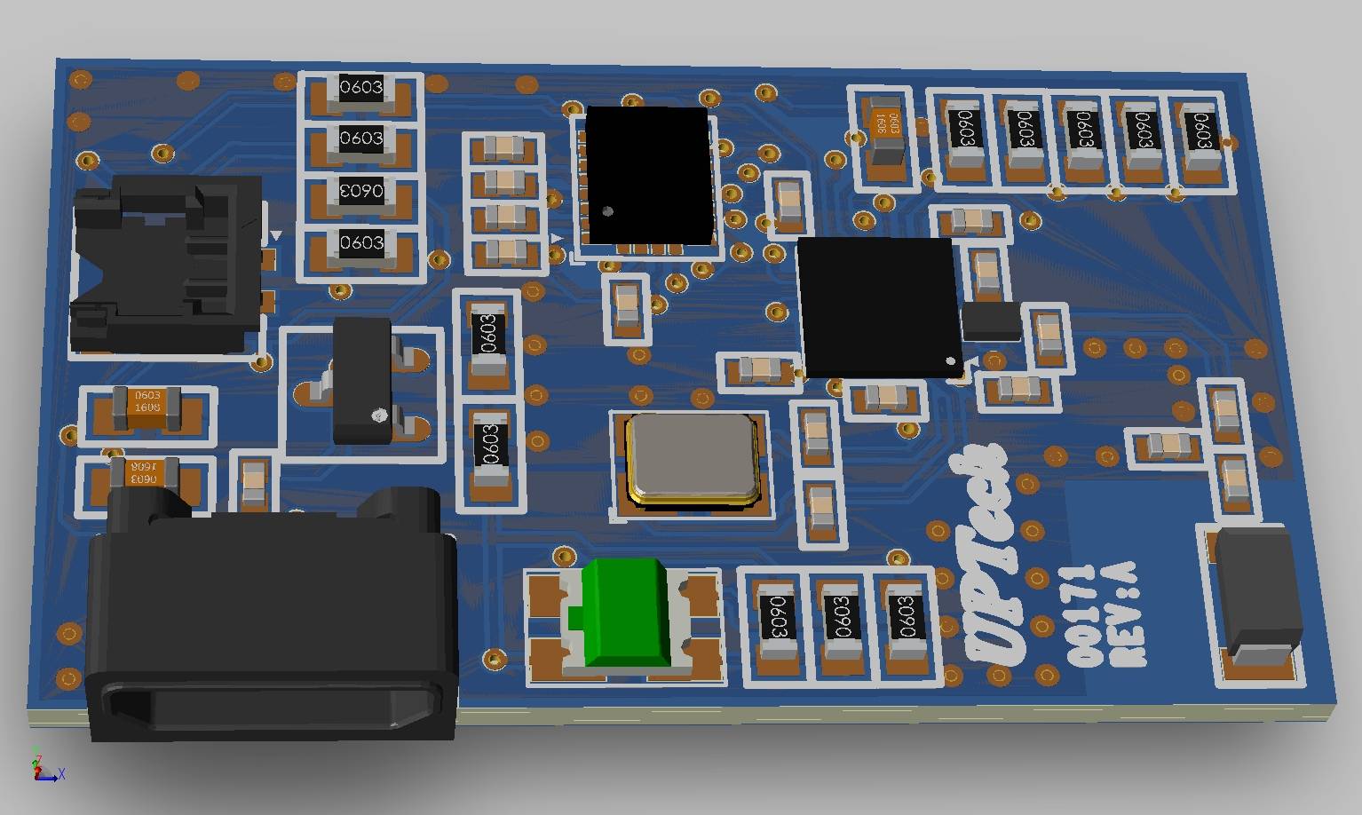
3D design, TOP side view
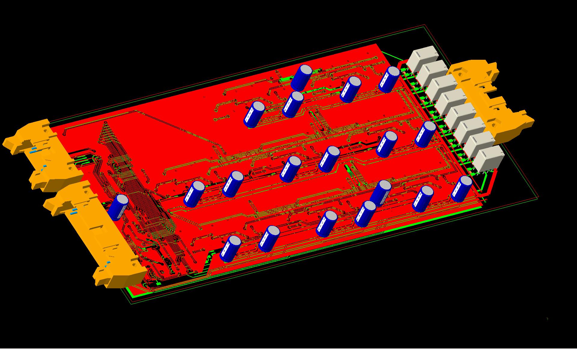
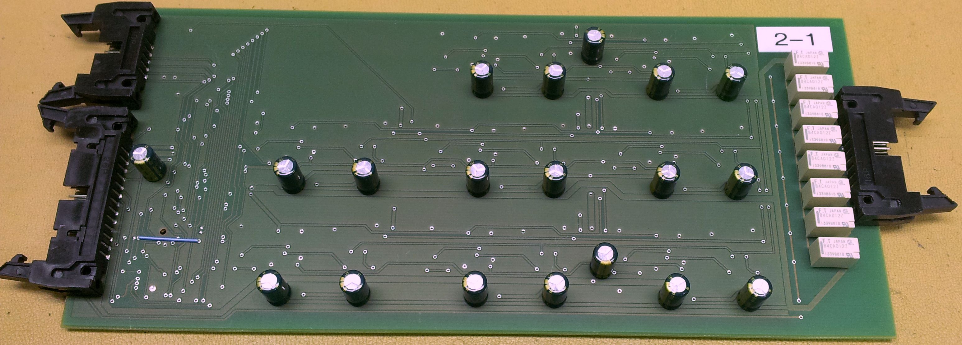
3D design, BOT side view
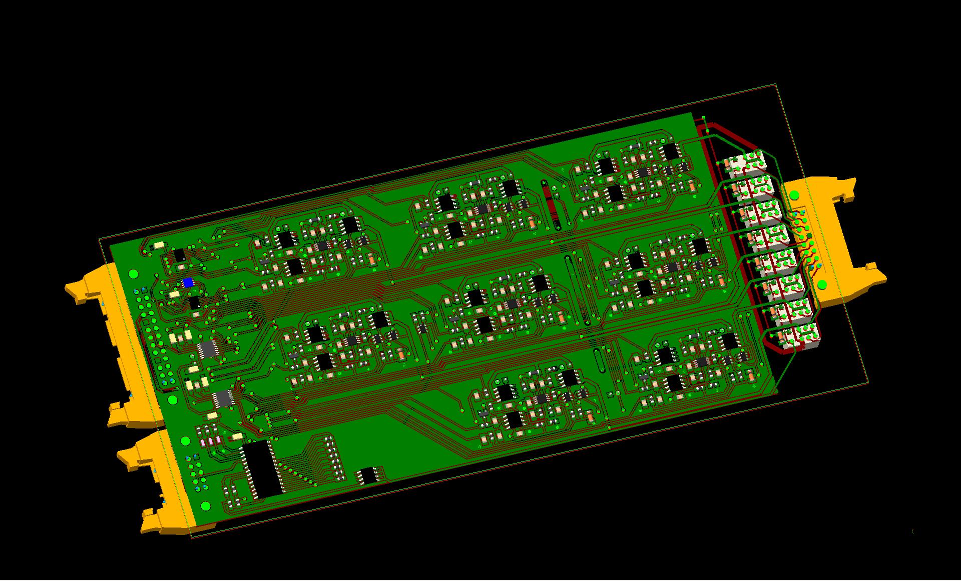
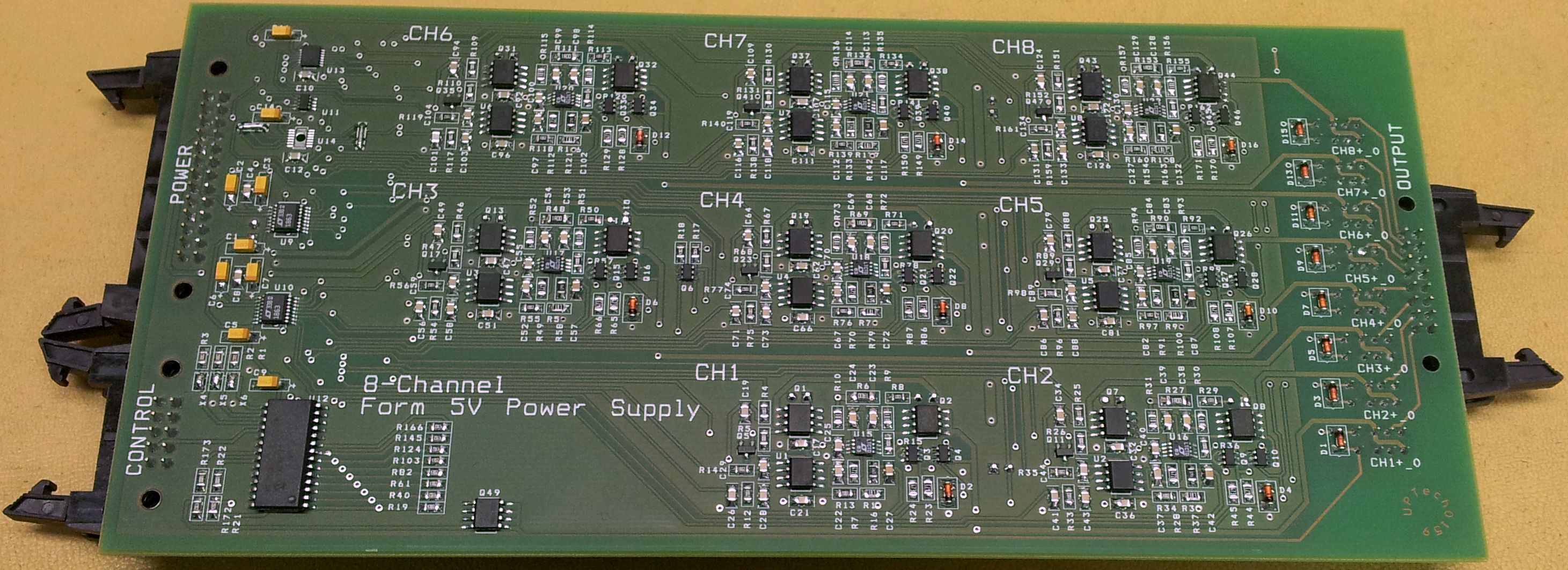
Hierarchical structure schematics
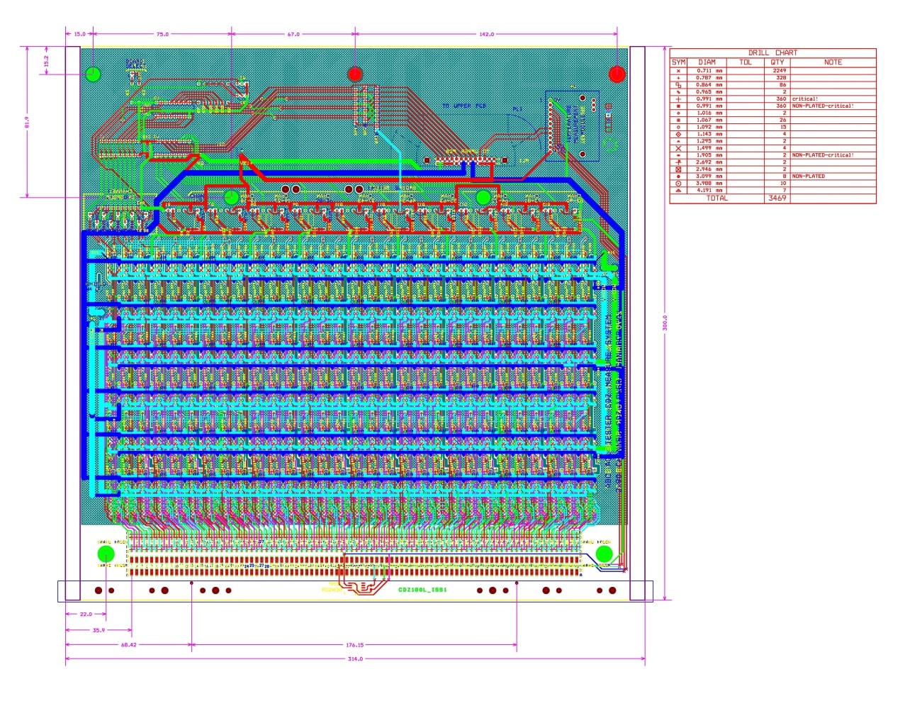
6 - layer PCB
|

|